1. Nanoelectronics
- Non-invasive atomic layer etching. A protocol
is devised that allows for non-invasive and atomically digital etching
of van der Waals transition-metal dichalcogenides through selective
alloying via low-temperature thermal diffusion and subsequent wet etching,
representing a highly precise and non-invasive tailoring route for material
manipulation. See
Nat. Commun. 13, 1844 (2022).
- An air-gapped FET. By using van der Waals
stacking method, we fabricated semi-suspended, ari-gapped FETs with
negligible scanning hystersis and high carrier mobilities. See Appl.
Phys. Lett. 121, 023503 (2022).
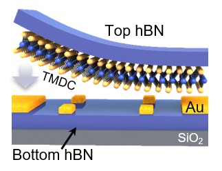
- Clean BN-Encapsulated 2D FETs. We managed
to integrate lithography-defined contacts into BN-encapsulated 2D FETs,
giving rise to high overall device quality comparable to the state-of-the-art
results. See ACS
AMI 14, 18697 (2022).
- On-chip integration of patterned 2D materials.
We developed an novel subsidence-assisted integration method that
enables spatially precise integration of arrays of micropatterned 2D
crystals onto Si/SiO2 substrates, representing an attractive, low-cost
system-on-chip strategy toward More-than-Moore microelectronics. See
ACS Nano. 13, 2654 (2019).
- Graphene voltage inverters. We exploited
the spontaneous surface passivation of Al to define the gate/dielectric
stacks and fabricated complementary-like voltage inverters based on
ambipolar graphene transistors, with over-unity voltage gains and matched
input and output. See Nano
Lett. 10, 2357 (2010);
ACS Nano.
5, 500 (2011); Small
7, 1552 (2011).
2. Device physics in FETs
- Theory of charge scattering. We developed
a generalized Coulomb scattering model with strictly considering device
configurative conditions, that is, asymmetric dielectric environments
and lopsided carrier distribution in 2D FETs, to accurately describe
the carrier scattering process [J.
Phys. Soc. Jpn., 84, 121011 (2015)] and the origin of the thinning-induced
mobility degradation [ Nano
Lett., 22, 6671(2022), Nano
Lett. 13, 3546 (2013)]. This understanding highlights the critical
role of surface quality in electrical transport. A review on charge
transport in 2D FETs can be found at Chem. Soc. Rev., 45,
118 (2016).
- Metal/Semiconductor contact. We investigated
the thickness scaling effect on the charge injection barrier at Au/MoS2
interfaces and observed the thickness reduction induced crossover of
electrical contact therein. [ACS
Nano, 8, 12836 (2014)]. In WS2 FETs with low-work-function
metal ytterbium (Yb) as contacts, we clarified the presence of significant
tunneling injection that invalidates the thermionic emission model for
barrier estimation. [Appl. Phys. Lett., 120,
253505 (2022)].
- Thickness identification of 2D crystals.
We observed strong optical inteference and its effect on Raman intensity
in the layered structures, which can be used to predict quantitative
Raman spectra and to count thickness of atomic layers on insulating
substrates. See ACS Nano, 6,
7381 (2012).